
TEC Science Class | Why is it harder to manufacture smaller refrigeration chips? A comprehensive guide to the materials, technologies, and structural challenges of micro-TEC
Driven by the rapid development of 5G communication, artificial intelligence and the Internet of Things, electronic devices are constantly evolving towards smaller, more compact and higher performance.Under this trend, the miniaturization of thermoelectric coolers has become an inevitable direction for industry development. This episode of Xiaocool will take you through the material, technological, and process challenges brought about by the miniaturization of thermoelectric coolers.
I. Challenges Brought by the Miniaturization of Thermoelectric Coolers
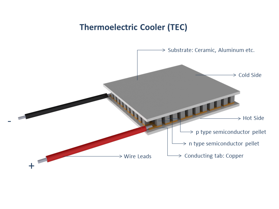
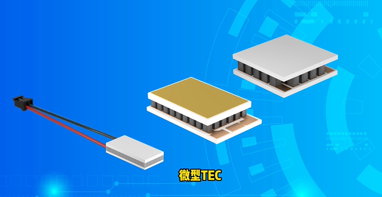
Microthermal condensers (TECs) are typically smaller than a fingernail (less than 5×5mm). Their interiors consist of numerous alternating P-type and N-type semiconductor particles, connected in series and parallel, much like "microcircuits," and soldered between two ceramic plates. As TEC sizes continue to shrink, increasing challenges arise in material selection, fabrication processes, and technology integration.
1.Thermoelectric materials encounter bottlenecks
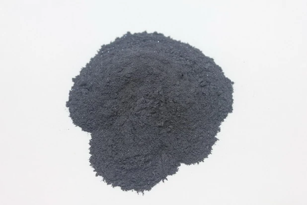
Bi₂Te₃ is currently the most commonly used thermoelectric material. It needs to be cut into tiny P - type and N-type semiconductor particles for assembling thermoelectric coolers. However , when the particle size reaches below 0.2 mm (approximately twice the diameter of a human hair), processing becomes extremely difficult, and the yield rate drops significantly. Furthermore, the shorter the particle size, the shorter the distance between the cold and hot ends, making it easier for heat to transfer directly from the hot end to the cold end, essentially creating a "hot-cold short circuit," resulting in a significantly worse cooling effect. For example, a thermoelectric cooler made with 0.2 mm particles will have a maximum temperature difference that is at least 10°C lower than one made with 0.6 mm particles.
Not only semiconductor particles, but ceramic substrates also face similar problems. The thickness of conventional ceramic sheets is between 0.15 and 0.25 mm. Although it can be reduced to 0.10 mm through grinding processes, the substrate size is too thin, which makes it prone to warping and cracking, and the yield rate will also decrease accordingly.
2.Manufacturing processes face challenges
The manufacturing process of microthermal chips is extremely delicate, with all steps requiring operation at the millimeter or even micrometer level. The smaller the chip, the more tightly packed the internal semiconductor particles are, with particle spacing potentially only tens of micrometers. At this level, even a slight misalignment can cause short circuits or misalignments between particles, leading to the failure of the entire device.
The manufacturing process for ceramic substrates is also challenging: typically, copper needs to be electroplated onto the ceramic surface as "pads" to connect semiconductor particles. As the size of the cooler shrinks, the distance between the pads also narrows—during electroplating, the copper layer can easily "grow too long," causing adjacent pads to connect and triggering a short circuit.
3.Structural strength and reliability issues
As the size of the thermoelectric cooler decreases, structural strength becomes a major issue. On the one hand, the soldering area of the entire device decreases, making the connections more fragile; on the other hand, the different materials used in the thermoelectric cooler (such as ceramics , semiconductors, and metal plating) expand at different rates when heated—leading to internal stress, which can easily cause cracks or even breakage at the semiconductor or plating.
Faced with these challenges, traditional designs and processes are no longer sufficient. To ensure the quality of miniature thermoelectric coolers, it is necessary to consider all aspects, including structural design, material matching, and manufacturing processes, and explore new ideas and methods to achieve a true breakthrough in the trend of miniaturization.
II. Solutions for Materials, Processes, and Structures
1.Materials Innovation
Researchers have successfully developed a superior thermoelectric material by improving the preparation method of bismuth telluride (Bi₂Te₃) crystal rods. New processes, such as annealing, hot forging, and adjusting the alloy composition, not only improved the material's thermoelectric conversion efficiency (thermoelectric figure of merit) but also enhanced its mechanical strength. The new material meets the high - performance requirements of micro-cooling chips while also adapting to the processing and usage needs of miniature sizes—it is more robust, more efficient, and more suitable for mass production.
2.Process Upgrade
To support the miniaturized production of thermoelectric coolers, the team specifically customized a series of automated equipment (automatic sorting machine + flexible placement machine) and upgraded the die identification and assembly system: controlling the placement accuracy error of semiconductor particles to within 10µm and the angular deviation to no more than 2°. At the same time, the circuit patterns on the ceramic substrate were significantly improved, allowing the line spacing to reach 50µm, fully meeting the application requirements of high-performance devices.
3.Structural Upgrade
Furthermore, by adjusting the conductivity of the semiconductor particles, structural designs of different sizes can be flexibly adapted. Even with the temperature cooler size reduced to 1×1mm, it maintains good mechanical strength and operational stability. Combined with a high-density plating process, the bonding force between material layers is further enhanced, ensuring the miniature temperature cooler remains reliable and durable after undergoing severe temperature cycling, meeting the GR-468 reliability standard of the communications industry.
FerroTec has successfully designed miniature thermoelectric coolers with dimensions of 1mm in length and width and 0.5mm in thickness, which are widely used in precision fields such as optical communication, lidar, and wearable devices. In the future, they will be embedded in even more high-tech products. For product details or to obtain solutions, please contact us at 0571-89712612.